Strong Inversion Region. Saturation cut-off and ohmic region.
Typical V I Characteristics Of Mosfets By Openstax Page 4 4 Jobilize
Important Points About The V-I Characteristics of SCR Forward Characteristics.

. When anode is positive wrt. The curve between drain current I D and drain-source voltage V DS of a JFET at constant gate-source voltage V GS is known as output characteristics of JFET. Field Effect Transistor Circuit Basics and Characteristics.
The output current is controlled by the input gate voltage. FET circuit design techniques are often used in overall circuit design. V ds 01 and V ds 1.
Both the plots have non zero current in the sub threshold region but Vds1 plot has a higher current due to the DIBL effect. When V GS is sufficiently positive and is larger than V TH then a large number of electrons are attracted under the age and the surface is said to be inverted. The parabolic nature of the curve can be seen in figure 8.
In fig1 OABC is the forward characteristics of SCR at I G 0. Cathode the curve between V and I is called the forward characteristics. The inversion layer full of electrons is now a connecting path between the two n-type source and drain regions.
Basics of N-Channel MOSFET Working and Characteristics. The reverse-biasing of the gate junction is not uniform throughout The reverse. N-Channel MOSFET is a type of metal oxide semiconductor field-effect transistor that is categorized under the field-effect transistors FET.
Ohmic or Linear Region. MOSFET transistor operation is based on the capacitor. The MOSFET operated in this region is said to be in weak inversion or the sub threshold region.
With the increase in drain current I D the ohmic voltage drop between the source and channel region reverse-biases the gate junction. Due to a nonzero V DS electrons flow from the drain to. When MOSFETs are made to operate in this region they are used as amplifiers.
The breakdown region is not included as it is not recommended for BJTs to operate in this region. Fig1ii shows the drain characteristic. In integrated circuits the.
These are able to provide characteristics that are not possible when using the more traditional bipolar transistors. MOSFET makes a very good capacitor when V GS V TH few hundred mV. The gate and the channel form a capacitor.
The characteristics of JFET is defined by a plotting a curve between the drain current and drain-source voltage. It is suitable for high power applications as it can withstand large amount of currents. The region below V t is called the sub threshold region.
This is also called as cut-off region. V DS V OV. The variation of drain current with respect to the voltage applied at drain-source terminals keeping the gate-source voltage constant is.
When MOSFETs are made to operate in this region they can be used as amplifiers. Hence the gate current controls the output drain. If V GS 0 then the depletion region of the channel is very small and in this region the JFET acts as a voltage controlled resistor.
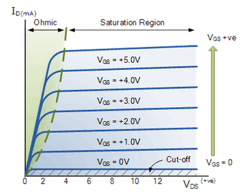
This type of transistor is also known as an insulated-gate field-effect transistor IGFET. The drain characteristics of a MOSFET are drawn between the drain current I D and the drain source voltage V DS. NMOS I-V Characteristic in Triode Region for V DS very close to zero.
Mainly the JFET operates in ohmic saturation cut-off and break-down regions. The device is on as the threshold has been crossed. The characteristic curve is as shown below for different values of inputs.
The JFET enters into this region when the gate voltage is large negative then the. As you can see in figure 4 there are three operating regions of a BJT cutoff region saturation region and active region. The graph shows the IV characteristics for two different V ds.
Hence the field created by the input gate. In the application where the MOSFET used as a switch the device works in the cut-off region and ohmic region when turned OFF and ON respectively. In this region MOSFET behaves like an open switch and is thus used when they are required to function as electronic switches.
Field effect transistors are used in many different areas of electronic circuit s. The slope of V DS-I D characteristics in this mode is called ON state resistance r DS of MOSFET. The graph for studying the characteristic curve of a field effect transistor_ FET is plotted between the varying values of Drain Current represented by ID along the y-axis with the varying values of VDS along.
NMOS I-V Characteristic in Triode Region ie. The plots in figure 8 and figure 9 show the IV characteristics of the NMOS that we have considered in its linear mode of operation. N Channel Enhancement type Mosfet characteristics and working.
The ohmic region is a region where the current I DSincreases with an increase in the value of V DS. It is a graph of drain current I d versus drain to source voltage V DS for different values of the gate to source voltage V GS. V CE curve for different values of I B.
In general any MOSFET is seen to exhibit three operating regions viz Cut-Off Region Cut-off region is a region in which the MOSFET will be OFF as there will be no current flow through it. Due to reduction of the channel resistance at higher values of V GS r DS reduces with increase in V GS. Mosfet is a three terminal device which is a type of FET Field effect transistor.
Saturation Region In saturation region the MOSFETs have their I DS constant inspite of an increase in V DS and occurs once V DS exceeds the value of pinch-off voltage V P. If the supply voltage is increased from zero a point reached point A when the SCR starts conducting. In the saturation region the MOSFETs have their I DS constant in spite of an increase in V DS and occurs once V DS exceeds the value of pinch-off voltage V P.
Operating Regions of the MOSFET MOSTransistorCharacteristics-LinearRegion Assume that V G V TN and V GS V TN V DS. It has three regions. At higher values of V DS I D tends to saturate with increase in V DS and this is called active region.
Ohmic or linear region is a region where in the current I DS increases with an increase in the value of V DS. This region to the left of the knee point of the curve is called the channel ohmic region because in this region the FET behaves like an ordinary resistor. Actually when V DS is increased the drain current I D should increase but due to the applied V GS the drain current is controlled at certain level.
Fig1 i shows the circuit diagram for determining the drain characteristic with shorted-gate for an n-channel JFET. Drain Characteristic With Shorted-Gate. Characteristics of FET The Current Voltage I-V characteristics of the Field Effect Transistor is plotted between the applied voltage VDS and Drain Current ID.
Characteristics Of Jfet Drain And Transfer Characteristics In English Youtube
![]()
Junction Field Effect Transistor Jfet N Channel Jfet Biasing V I

Mosfet Characteristics Vi And Output Characteristics Electrical4u


0 Comments